Impedans Langmuir Probes are a versatile tool in every plasma assisted deposition and etching process. To control and fine tune the process, Langmuir Probe provides real time information about the crucial plasma parameters such as electron density, temperature, plasma potential and EEFDF. These measurements provide insights into the tool performance enabling correlation of process parameters with the key performance metrics like etch rate and selectivity in an etching process.
A recent publication in Journal of Vacuum Science and Technology A highlights the application of Impedans Langmuir probe in the etching of a magnetic tunnel junction layer of magnetic random-access memory (MRAM). The Langmuir Probe measurements played a key role in understanding the function of plasma species to improve the etch rate and selectivity at different RF bias conditions.
A schematic diagram of the rf-biased reactive ion beam etching system used in the experiment is shown in figure 1. For the reactive ion beam, an inductively coupled plasma (ICP) source operated with 13.56 MHz was installed at the top of the processing chamber. The reactive ions were extracted and accelerated from the ICP ion beam source to the processing chamber through a grid assembly consisting of three grids made of molybdenum
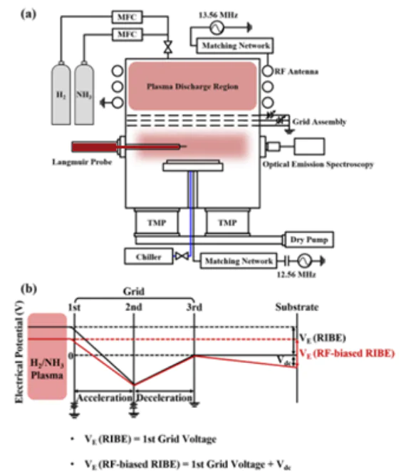
Figure 1 (a) Schematic diagram of the rf-biased reactive ion beam etching system. (b) Electrical potentials VE between the ion source and the substrate during RIBE and rf-biased RIBE. The net electrical potential is first grid voltage + Vdc (for RIBE, Vdc = 0).
A positive and negative voltage was applied to the first and second grid to control the energy and flux of the ions respectively, keeping the ground potential to the third grid. The substrate was grounded or negatively biased by applying 12.56 MHz rf power to the substrate for the operation as RIBE and rf-biased RIBE, respectively.
MRAM materials such as CoFeB and MgO and mask materials such as the hardmask (HM) and the top electrode (TE) were sputter deposited on Si wafers. In addition, an MTJ structure of CoFeB/MgO/CoFeB deposited on bottom electrode (BE)/Si wafers was dot-patterned with a mask of HM/TE. For etching, gas mixtures composed of H2/NH3 were used at 1 mTorr of pressure in the process chamber and the substrate was kept at 20 °C. A single Langmuir probe was used to measure the plasma density above the substrate in RF biased conditions.
The etch rates and selectivities of MTJ and mask materials were measured for different −Vdc to the substrate while maintaining the same electrical potential differences of ∼250 V by varying the first grid voltage together with −Vdc. As shown in fig. 2(a), the increase in −Vdc decreased the etch rates slowly. It is possibly due to the decreased ion flux extracted from the ion beam source at the lower first grid voltage. However, as shown in fig. 2(b) when a low −Vdc of approximately −20 V was applied to the substrate, the etch selectivities of CoFeB/TE and MgO/TE were increased significantly even though the further increase in −Vdc to −100 V decreased the etch selectivity.
The etch selectivities of MTJ/HM, were generally lower than 1, and no significant changes with increasing −Vdc were observed. The further increase in −Vdc not only decreased the etch rates of MTJ materials but also decreased the etch selectivity of MTJ/TE. It is believed that the lower etch rates are related to the lower ion flux from the ion beam source by using the lower first grid voltage for higher −Vdc. Also, the lower etch selectivity with increasing −Vdc at the same electrical potential of first grid V/−Vdc might be related to the increased high energy ion flux for higher −Vdc.
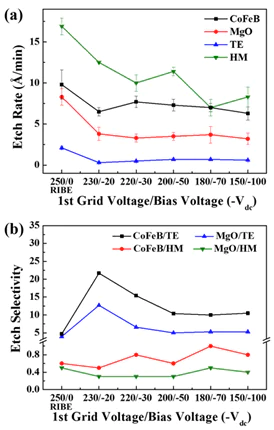
Figure 2 (a) Etch rates of MTJ and hard mask materials and (b) etch selectivities of MTJ materials over mask materials of TE and HM according to different first grid V/−Vdc ratios while maintaining the total electrical potential fixed at ∼250 V.
The change in plasma density during rf-biased RIBE was observed using a Langmuir probe, and is shown in fig. 3. Even though the plasma density is very low in the range of 108–109/cm3 due to the low rf power of 35 – 60 W, the plasma density was slowly increased with increasing −Vdc. The increase in −Vdc by increasing rf-bias power also increases the ion energy distribution to the substrate; therefore, higher energy ions to the substrate can be obtained with increasing −Vdc at the same first grid V/−Vdc and which increases the physical sputter etching effect.
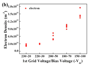
Figure 3 Electron density measured by a Langmuir probe
Langmuir Probe measurements helped to improve etch characteristics of the MTJ layer of the MRAM using RIBE processing. When a small rf-biasing (−Vdc = −20V) was added to a RIBE condition while maintaining the ion bombardment energy to the substrate similar (by decreasing the first grid voltage from the ion beam while increasing −Vdc to the substrate by rf-biasing), the highest etch selectivity of MTJ over TE was obtained.
Utilizing Impedans’ Langmuir probe to measure electron density reaching on the electrode offer insights into the etching process. Consequently, control over the etch selectivity and etch rates can be achieved through manipulation of RF bias voltages.
To know more about Impedans Langmuir Probes click here.
To download the summary of the paper click here
Reference
Reference Ye Eun Kim al. et al, Study on etch characteristics of magnetic tunnel junction materials using rf-biased H2 /NH3 reactive ion beam. J. Vac. Sci. Technol. A 41, 033005 (2023)